- Products & Capabilities

- About
- Resources
Electrical Testing for PCB and PCBA: The Role of Flying Probe Testing


Flying Probe Testing ensures high-performance, durable PCBs and PCBAs by detecting issues like shorts and capacitance mismatches, speeding up production, and reducing costs.
Because production packaging demands higher performance and durability from the final goods, not only bare PCBs but also PCBAs must be tested while they are still in the shop before shipping. Electrical tests are performed to detect potential problems including resistance, capacitance mismatches, openings, and shorts, ensuring that both bare and populated boards are manufactured appropriately.
Evolution and Significance
The flying probe test, which was first only used for bare board inspections, has nearly entirely evolved to be used for assembled and bare boards as well. This has drastically changed test methodologies for low-volume, fast-turnaround assembly products, cutting down on product design cycles and speeding up time to market.
What is Flying Probe Testing?
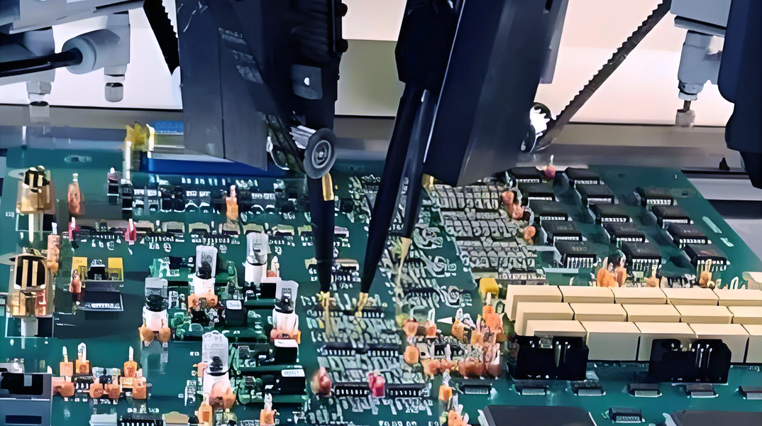
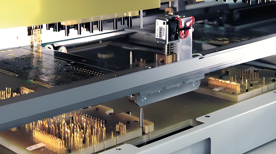
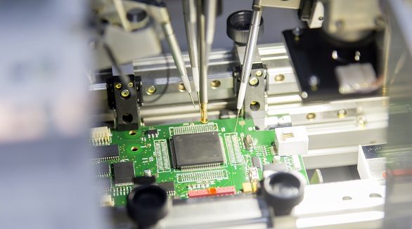
The flying probe testing can be regarded as an advanced version of the bed-of-nails fixture test, using moving probes instead of fixed pins, and a flying probe tester houses four headers along the X-Y axis, which are capable of high-speed movement.
The Unit Under Test is used against the internal tester during the test. Test pads and vias, which are in charge of finding defects in the UUT, come into touch with probes. They are routed to drivers (sensations) through a multiplexing system, such as signal generators, power supplies, digital multimeters, and frequency counters, enabling stimulation of all the components on the UUT. All the components that are not under the test are shielded to curb the interference of data.
Shorts open, and component values may be verified using the flying probe tester. Added to that, it is equipped with a camera that identifies missing components and confirms component polarity. Flying probe testers support positioning accuracy and repeatability in the order of 5μm to 15μm. With this kind of accuracy, flying probe testers can evaluate the fabrication quality of the UUT.
Bed of Nails Test vs. Flying Probe Test
The flying probe test beats the bed-of-nails testing, especially in PCB assembly testing, reducing the test development cycle, enabling faster market entry for products. Moreover, the bed of nails test no longer requires fittings, which lowers expenses. Prototypes may be tested quickly and affordably in low numbers, thanks to the convenient nature of testing.
Working Principles
Compared to traditional ICT (In-Circuit Testing) methods, flying probe testing is simpler to use and may save time. The testing crew converts the CAD (Computer-Aided Design) data into a format that can be used as a testing program. In order to meet the UUT standards, the test program and physical nets created using new files are then constructed.
After the test programming is complete, the physical flying probe test exercise begins. A test such as shorts is chosen, then reference points from the CAD data about the chosen test are identified. The UUT is mounted on the platform and the resulting test that is developed is run. This brings out issues regarding fabrication or assembly.
Debugging is a crucial phase that comes before actual testing. Flying probe testing debugs far much faster compared to the conventional ICT test setup.
Advantages of Flying Probe Test
A short test development cycle and relatively low testing costs.
High conversion flexibility.
Rapid feedback to both the PCB design engineers and fabricators was obtained at the prototype stage.
Flying probe testing requires less time for testing in total compared to conventional ICT. It is possible to initiate PCB assembly with the CAD file received in a matter of hours and test prototype assemblies just after they have been assembled. This is far from the experience with conventional ICT, which may consume months before such tests. Even general technicians can operate a flying probe test system since the setup, programming, and execution of tests are relatively easy.
Disadvantages of Flying Probe Test
While there are many advantages to flying probe testing, this method also has some disadvantages. The fact that the pins of the probes are in physical contact with the vias and test pads causes the board surface to have some minor pits that can be treated as fabrication defects by some OEMs. In this way, technology is being continuously improved to address this problem.
With the components that have no test pads, the probes might only contact the leads of the components and would miss possible problems such as loose leads or connections that were soldered poorly.
Nonetheless, such advantages aside, flying probe testing is still an indispensable process in the printed circuit board fabrication and assembly process, playing a crucial role in ensuring the performance and reliability of electronic products.
Hot Tags:
Contact us

If you can't find what you're looking for, please contact us.
 2024/08/01